- 您现在的位置:买卖IC网 > Sheet目录328 > IDT70T3339S200BCG (IDT, Integrated Device Technology Inc)IC SRAM 9MBIT 200MHZ 256BGA
IDT70T3339/19/99S
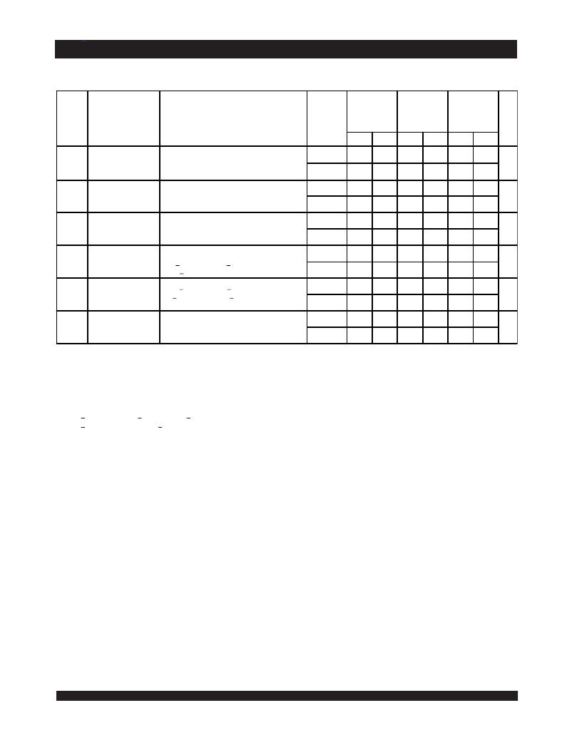
High-Speed 2.5V 512/256/128K x 18 Dual-Port Static RAM
Industrial and Commercial Temperature Ranges
DC Electrical Characteristics Over the Operating
Temperature and Supply Voltage Range (3) (V DD = 2.5V ± 100mV)
70T3339/19/99
S200
Com'l Only (8)
70T3339/19/99
S166
Com'l
& Ind (7)
70T3339/19/99
S133
Com'l
& Ind
Symbol
Parameter
Test Condition
Version
Typ. (4)
Max.
Typ. (4)
Max.
Typ. (4)
Max.
Unit
I DD
Dynamic Operating
CE L and CE R = V IL ,
COM'L
S
375
525
320
450
260
370
Current (Both
Outputs Disabled,
mA
Ports Active)
f = f MAX (1)
IND
S
___
___
320
510
260
450
I SB1 (6)
Standby Current
CE L = CE R = V IH
COM'L
S
205
270
175
230
140
190
(Both Ports - TTL
f = f MAX (1)
mA
Level Inputs)
IND
S
___
___
175
275
140
235
I SB2 (6)
Standby Current
CE "A" = V IL and CE "B" = V IH (5)
COM'L
S
300
375
250
325
200
250
(One Port - TTL
Active Port Outputs Disabled,
mA
Level Inputs)
f=f MAX (1)
IND
S
___
___
250
365
200
310
I SB3
Full Standby Current
Both Ports CE L and
COM'L
S
5
15
5
15
5
15
(Both Ports - CMOS
CE R > V DDQ - 0.2V, V IN > V DDQ - 0.2V
mA
Level Inputs)
or V IN < 0.2V, f = 0 (2)
IND
S
___
___
5
20
5
20
I SB4 (6)
Full Standby Current
CE "A" < 0.2V and CE "B" > V DDQ - 0.2V (5)
COM'L
S
300
375
250
325
200
250
(One Port - CMOS
V IN > V DDQ - 0.2V or V IN < 0.2V
mA
Level Inputs)
Active Port, Outputs Disabled, f = f MAX (1)
IND
S
___
___
250
365
200
310
Izz
Sleep Mode Current
ZZ L = ZZ R = V IH
COM'L
S
5
15
5
15
5
15
(Both Ports - TTL
f=f MAX (1)
mA
Level Inputs)
IND
S
___
___
5
20
5
20
NOTES:
5652 tbl 09
1. At f = f MAX , address and control lines (except Output Enable) are cycling at the maximum frequency clock cycle of 1/t CYC , using "AC TEST CONDITIONS".
2. f = 0 means no address, clock, or control lines change. Applies only to input at CMOS level standby.
3. Port "A" may be either left or right port. Port "B" is the opposite from port "A".
4. V DD = 2.5V, T A = 25°C for Typ, and are not production tested. I DD DC (f=0) = 15mA (Typ).
5. CE X = V IL means CE 0X = V IL and CE 1X = V IH
CE X = V IH means CE 0X = V IH or CE 1X = V IL
CE X < 0.2V means CE 0X < 0.2V and CE 1X > V DDQ - 0.2V
CE X > V DDQ - 0.2V means CE 0X > V DDQ - 0.2V or CE 1X - 0.2V
"X" represents "L" for left port or "R" for right port.
6. I SB1 , I SB2 and I SB4 will all reach full standby levels (I SB3 ) on the appropriate port(s) if ZZ L and/or ZZ R = V IH .
7. 166MHz I-Temp is not available in the BF-208 package.
8. 200Mhz is not available in the BF-208 package.
9
6.42
发布紧急采购,3分钟左右您将得到回复。
相关PDF资料
IDT70T3509MS133BP
IC SRAM 36MBIT 133MHZ 256BGA
IDT70T3519S133DRI
IC SRAM 9MBIT 133MHZ 208QFP
IDT70T3539MS166BCG
IC SRAM 18MBIT 166MHZ 256BGA
IDT70T3719MS166BBG
IC SRAM 18MBIT 166MHZ 324BGA
IDT70T633S10BCI
IC SRAM 9MBIT 10NS 256BGA
IDT70T651S12DRI
IC SRAM 9MBIT 12NS 208QFP
IDT70T653MS12BCI
IC SRAM 18MBIT 12NS 256BGA
IDT70V05L55G
IC SRAM 64KBIT 55NS 68PGA
相关代理商/技术参数
IDT70T3399S133BC
功能描述:IC SRAM 2MBIT 133MHZ 256BGA RoHS:否 类别:集成电路 (IC) >> 存储器 系列:- 标准包装:3,000 系列:- 格式 - 存储器:EEPROMs - 串行 存储器类型:EEPROM 存储容量:8K (1K x 8) 速度:400kHz 接口:I²C,2 线串口 电源电压:1.7 V ~ 5.5 V 工作温度:-40°C ~ 85°C 封装/外壳:8-SOIC(0.154",3.90mm 宽) 供应商设备封装:8-SOIC 包装:带卷 (TR)
IDT70T3399S133BC8
功能描述:IC SRAM 2MBIT 133MHZ 256BGA RoHS:否 类别:集成电路 (IC) >> 存储器 系列:- 标准包装:3,000 系列:- 格式 - 存储器:EEPROMs - 串行 存储器类型:EEPROM 存储容量:8K (1K x 8) 速度:400kHz 接口:I²C,2 线串口 电源电压:1.7 V ~ 5.5 V 工作温度:-40°C ~ 85°C 封装/外壳:8-SOIC(0.154",3.90mm 宽) 供应商设备封装:8-SOIC 包装:带卷 (TR)
IDT70T3399S133BCI
功能描述:IC SRAM 2MBIT 133MHZ 256BGA RoHS:否 类别:集成电路 (IC) >> 存储器 系列:- 标准包装:3,000 系列:- 格式 - 存储器:EEPROMs - 串行 存储器类型:EEPROM 存储容量:8K (1K x 8) 速度:400kHz 接口:I²C,2 线串口 电源电压:1.7 V ~ 5.5 V 工作温度:-40°C ~ 85°C 封装/外壳:8-SOIC(0.154",3.90mm 宽) 供应商设备封装:8-SOIC 包装:带卷 (TR)
IDT70T3399S133BCI8
功能描述:IC SRAM 2MBIT 133MHZ 256BGA RoHS:否 类别:集成电路 (IC) >> 存储器 系列:- 标准包装:3,000 系列:- 格式 - 存储器:EEPROMs - 串行 存储器类型:EEPROM 存储容量:8K (1K x 8) 速度:400kHz 接口:I²C,2 线串口 电源电压:1.7 V ~ 5.5 V 工作温度:-40°C ~ 85°C 封装/外壳:8-SOIC(0.154",3.90mm 宽) 供应商设备封装:8-SOIC 包装:带卷 (TR)
IDT70T3399S133BF
功能描述:IC SRAM 2MBIT 133MHZ 208FBGA RoHS:否 类别:集成电路 (IC) >> 存储器 系列:- 标准包装:3,000 系列:- 格式 - 存储器:EEPROMs - 串行 存储器类型:EEPROM 存储容量:8K (1K x 8) 速度:400kHz 接口:I²C,2 线串口 电源电压:1.7 V ~ 5.5 V 工作温度:-40°C ~ 85°C 封装/外壳:8-SOIC(0.154",3.90mm 宽) 供应商设备封装:8-SOIC 包装:带卷 (TR)
IDT70T3399S133BF8
功能描述:IC SRAM 2MBIT 133MHZ 208FBGA RoHS:否 类别:集成电路 (IC) >> 存储器 系列:- 标准包装:3,000 系列:- 格式 - 存储器:EEPROMs - 串行 存储器类型:EEPROM 存储容量:8K (1K x 8) 速度:400kHz 接口:I²C,2 线串口 电源电压:1.7 V ~ 5.5 V 工作温度:-40°C ~ 85°C 封装/外壳:8-SOIC(0.154",3.90mm 宽) 供应商设备封装:8-SOIC 包装:带卷 (TR)
IDT70T3399S133BFI
功能描述:IC SRAM 2MBIT 133MHZ 208FBGA RoHS:否 类别:集成电路 (IC) >> 存储器 系列:- 标准包装:3,000 系列:- 格式 - 存储器:EEPROMs - 串行 存储器类型:EEPROM 存储容量:8K (1K x 8) 速度:400kHz 接口:I²C,2 线串口 电源电压:1.7 V ~ 5.5 V 工作温度:-40°C ~ 85°C 封装/外壳:8-SOIC(0.154",3.90mm 宽) 供应商设备封装:8-SOIC 包装:带卷 (TR)
IDT70T3399S133BFI8
功能描述:IC SRAM 2MBIT 133MHZ 208FBGA RoHS:否 类别:集成电路 (IC) >> 存储器 系列:- 标准包装:3,000 系列:- 格式 - 存储器:EEPROMs - 串行 存储器类型:EEPROM 存储容量:8K (1K x 8) 速度:400kHz 接口:I²C,2 线串口 电源电压:1.7 V ~ 5.5 V 工作温度:-40°C ~ 85°C 封装/外壳:8-SOIC(0.154",3.90mm 宽) 供应商设备封装:8-SOIC 包装:带卷 (TR)
